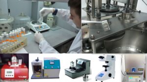
The laboratory focuses on the synthesis of semiconductor materials of various types (two-, three-, four-component, doped materials, solid solutions) with special attention to process control during synthesis, annealing, pressing, etc.
Directions:
- synthesis and characterization of semiconductor materials of various types (two-, three-, four-component, doped materials, solid solutions);
- PVD deposition of semiconductor thin films (deposition under vacuum thermal evaporation);
- measurement of thermoelectric parameters of materials (Seebeck coefficient, electrical conductivity, carrier concentration)
Equipments
- Hi Cube Pfeiffer vacuum post;
- Muffle furnace Nabertherm L 15 / 13;
- Auto pellet press 25 ton;
- Circular cutting machine Cutting Micracut 201 and Special stand with rotation for circular cutting machine;
- Planetary ball mills, Pulverisette 6;
- Analytical sieving machine and a set of sieve
s for a ball mill model AS 200 - Smart2pure water purification system;
- Hardness meter NEXUS 412A
- Vacuum post (VUP-5, UA) – deposition under vacuum thermal evaporation
- Vacuum post (VUP-5M, UA) – deposition under magnetron sputtering
- Devices for measuring thermoelectric parameters of materials – our own patented development (Seebeck coefficient, electrical conductivity, Hall mobility)
Contact: lyubomyr.nykyruy@pnu.edu.ua
